News Posts matching #Intel 18A

Return to Keyword Browsing

Intel Core Ultra "Panther Lake" Processor Hands-on and Up Close at Computex 2025

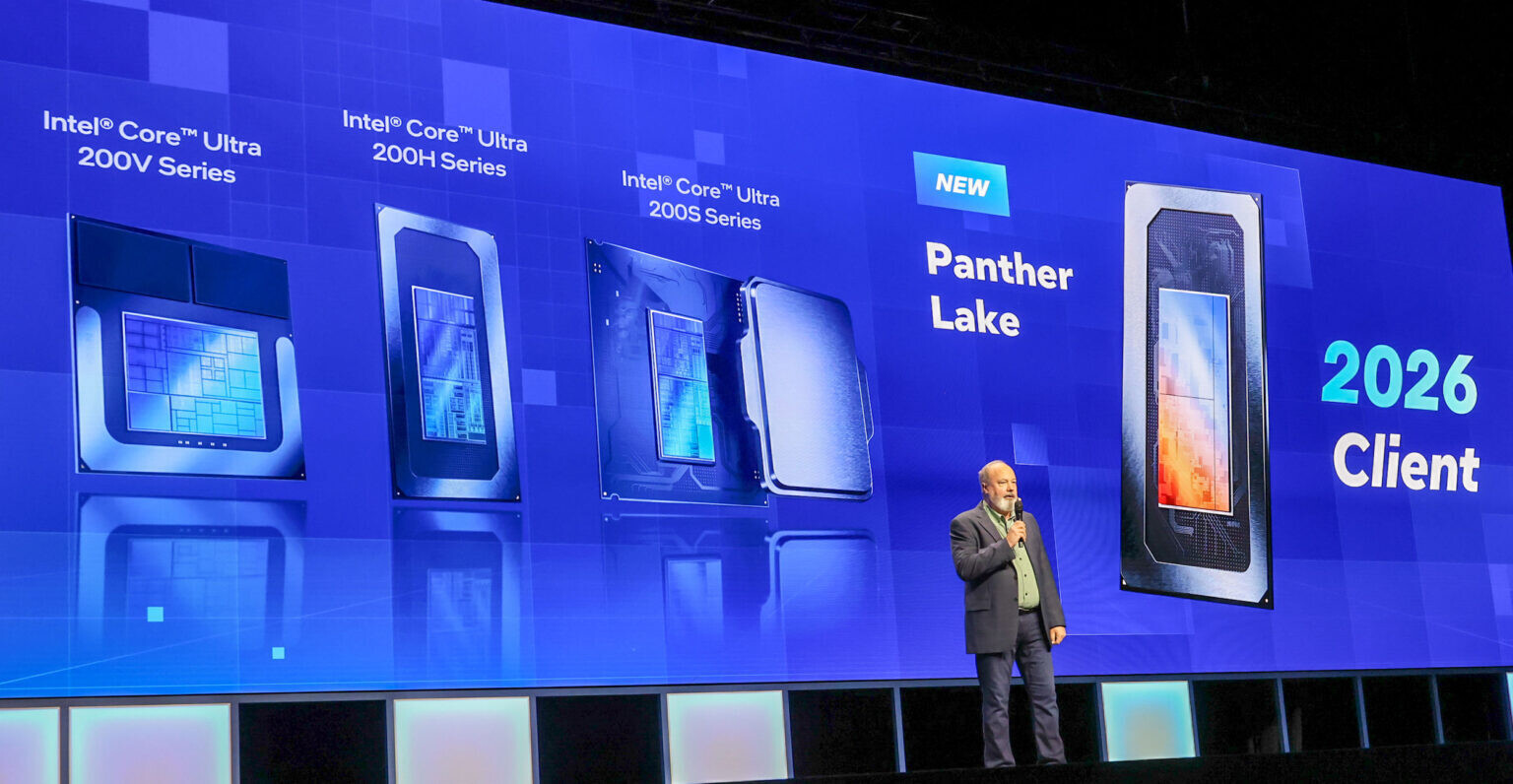
Intel at the 2025 Computex showed off its next-generation Core Ultra Series 3 processor, codenamed "Panther Lake." The mobile H-segment version of the chip comes with a slender rectangular package similar to "Arrow Lake-H" and "Meteor Lake." It is a tile-based disaggregated processor, but comes in a unique arrangement of tiles we haven't seen with the past two generations. The chip is dominated by two large tiles, one is very likely the Graphics + SoC tile, the smaller of the two being the Compute tile with the CPU cores, and the slender rectangular tiles being related to I/O.

As for IP, "Panther Lake" introduces a new generation iGPU powered by the Xe3 "Celestial" graphics architecture. The CPU complex consists of "Cougar Cove" P-cores, and "Darkmont" E-cores, both of which are expected to provide generational IPC improvements over the current "Lion Cove" and "Skymont." At Computex, we not only got to go hands-on with the mobile packages of "Panther Lake," but also see the chip in action, installed on a testing and platform validation system. The engineering goal with "Panther Lake," Intel says, is to offer efficiency similar to "Lunar Lake," but with performance generationally exceeding "Arrow Lake-H." The Compute tile is expected to be built on the new Intel 18A foundry node. Intel says "Panther Lake" is on track for mass-production in the second half of 2025, with the first consumer products expected at CES 2026.

Siemens and Intel Foundry Collaborates on Integrated Circuits and Advanced Packaging Solutions for 2D and 3D IC

Siemens Digital Industries Software today announced that its continued collaboration with Intel Foundry has resulted in multiple product certifications, updated foundry reference flows, and additional technology enablement leveraging the foundry's leading-edge technologies for next-generation integrated circuits (IC) and advanced packaging. Siemens is a founding partner of the Intel Foundry Accelerator Chiplet Alliance - enabling a new and compelling solution for 3D IC and chiplet offerings to a breadth of semiconductor market verticals.

Intel 18A Certification Achievements
Siemens' industry-leading Calibre nmPlatform tool is now certified for the latest Intel 18A production Process Design Kit (PDK). Intel 18A represents a significant technological leap forward, featuring innovative RibbonFET Gate-all-around transistors and the industry's first PowerVia backside power delivery. This Calibre certification allows mutual customers to continue leveraging the Calibre nmPlatform tool as their industry-standard sign-off solution with Intel Foundry's most advanced manufacturing process, accelerating time-to-market for next-generation chip designs.

Intel Foundry Gathers Customers and Partners, Outlines Priorities

Today at Intel Foundry Direct Connect, the company will share progress on multiple generations of its core process and advanced packaging technologies. The company will also announce new ecosystem programs and partnerships, and welcome industry leaders to discuss how a systems foundry approach enables collaboration with partners and unlocks innovation for customers.

Intel CEO Lip-Bu Tan will open the event by discussing Intel Foundry's progress and priorities as the company drives the next phase of its foundry strategy. Naga Chandrasekaran, Intel Foundry chief technology and operations officer, and Kevin O'Buckley, general manager of Foundry Services, will also deliver keynotes during the morning session, sharing process and advanced packaging news while highlighting Intel Foundry's globally diverse manufacturing and supply chain.

Synopsys & Intel Foundry Collaborate on Angstrom-Scale Chips - Using 18A & 18A-P Technologies

At today's Intel Foundry Direct Connect 2025 event, Synopsys, Inc. announced broad EDA and IP collaborations with Intel Foundry, including availability of its certified AI-driven digital and analog design flows for the Intel 18A process node and production-ready EDA flows for the Intel 18A-P process node with RibbonFET Gate-all-around transistor architecture and the industry's first commercial foundry implementation of PowerVia backside power delivery. To drive multi-die design innovation forward, Synopsys and Intel Foundry are collaborating to enable Intel's new Embedded Multi-die Interconnect Bridge-T (EMIB-T) advanced packaging technology with an EDA reference flow powered by Synopsys 3DIC Compiler. With its EDA flows, multi-die solution, and broad portfolio of Synopsys' foundation and interface IP on Intel 18A and Intel 18A-P, Synopsys is helping designers accelerate the development of highly optimized AI and HPC chip designs from silicon to systems.

In a keynote presentation at today's event, John Koeter, Senior Vice President, for the Synopsys IP Group, emphasized: "The successful collaboration between Synopsys and Intel Foundry is advancing the semiconductor industry with silicon to system design solutions to meet the evolving needs for AI and high-performance computing applications. Our production-ready EDA flows, IP, and multi-die solution, provides our mutual customers with comprehensive technologies to accelerate the development of chip designs that meet or exceed their requirements."

Cadence Expands Design IP Portfolio Optimized for Intel 18A and Intel 18A-P Technologies

Cadence today announced a significant expansion of its portfolio of design IP optimized for Intel 18A and Intel 18A-P technologies and certification of Cadence digital and analog/custom design solutions for the latest Intel 18A process design kit (PDK). These advancements are being showcased today at Intel Foundry Direct Connect, underscoring Cadence's continued leadership in driving industry innovation for artificial intelligence and machine learning (AI/ML), high-performance computing (HPC) and advanced mobility applications through its strategic partnership with Intel Foundry.

Cadence has collaborated closely with Intel Foundry to design and optimize a comprehensive range of solutions that fully leverage the innovative features of the Intel 18A/18A-P nodes, including RibbonFET Gate-all-around transistors and PowerVia backside power delivery network. With this collaboration, joint customers can achieve exceptional power, performance and area (PPA) efficiencies, accelerating time to market for cutting-edge system-on-chip (SoC) designs.

Intel's Biggest Foundry Customer Is Intel Itself—Fueled by "Intel 7" Node

Intel just reported its Q1 revenue results, and there are several interesting highlights from the earnings call. Intel Foundry, long touted for a comeback, is generating most of its revenue from a single customer, and it isn't the latest node. Intel's biggest customer is actually itself, predominantly using the "Intel 7" node (Intel's name for its 10 nm SuperFin process), which underpins the Alder Lake and Raptor Lake consumer CPU generations as well as the Sapphire Rapids Xeon server generation. As Intel ramps up 18A-node production and external clients begin testing their ASIC designs, 18A still isn't the Foundry division's primary revenue driver. Instead, demand for Intel 7 wafers is being fueled by massive orders for Intel's 13th- and 14th-generation Raptor Lake processors.

During the Q1 earnings call, Intel CFO Dave Zinsner noted, "Intel Foundry delivered revenue of $4.7 billion, up 8% sequentially on pull-ins of Intel 7 wafers and increased advanced packaging services." He also commented on the Q1 Foundry operating loss of $2.3 billion, attributing it to "startup costs associated with the ramp of products on Intel 18A." While the 18A node is gradually scaling to volume production for upcoming internal and external products, older nodes continue to fuel the revenue stream. Zinsner further confirmed that "we have a lot of important building blocks in place, including the ramp of Intel 18A in the second half of 2025 to support the launch of our first Panther Lake SKU by year-end, with additional SKUs coming in the first half of 2026."

Intel's 18A Node Outperforms TSMC N2 and Samsung SF2 in 2 nm Performance Class

Intel's 18A node isn't all about yields and density (which are still very important factors) but also performance. According to Taiwanese media 3C News, citing TechInsights research and calculations, the new leader of node performance is Intel 18A. On a custom scale used by TechInsights, Intel 18A gets a 2.53 score, while the performance score of TSMC N2 is 2.27, and the performance score of Samsung SF2 is 2.19. This is all among two nm-class nodes, where Intel leads the category. Being the first node with a Backside Power Delivery Network (BSPDN), it will appear in the Panther Lake CPUs in late 2025 for testing and early 2026 for shipments. This new power architecture boosts layout efficiency and component utilization by 5-10%, lowers interconnect resistance, and enhances ISO power performance by up to 4%, thanks to a significant drop in intrinsic resistance versus traditional front‑end power routing. Relative to its predecessor, Intel 3, the 18A process delivers a 15% improvement in performance per watt and packs 30% more transistors into the same area.

Featuring RibbonFET design, it has entered risk production. According to Intel, "This final stage is about stress-testing volume manufacturing before scaling up to high volume in the second half of 2025." When it comes to other aspects like SRAM density, high‑performance SRAM cells shrank from 0.03 µm² in Intel 3 to 0.023 µm² in Intel 18A, while high‑density cells contracted to 0.021 µm², reflecting scaling factors of 0.77 and 0.88 respectively and defying previous assumptions that SRAM scaling had plateaued. Intel's innovative "around‑the‑array" PowerVia approach addresses voltage drops and interference by routing power vias to I/O, control, and decoder circuits, freeing up the bit‑cell area from frontal power supplies. The result is a 38.1 Mbit/mm² macro bit density, positioning Intel to rival TSMC's N2. All this, combined with BSPDN, is shaping up a powerful node. We can't wait to get our hands on some 18A silicon in the future and run it through our labs for testing.

Intel Vision Presentation Labels Core Ultra 300 "Panther Lake" CPU Series as 2026 Products

Intel's freshly concluded Vision 2025 "Products Update and GTM" showcase included a segment dedicated to forthcoming Core Ultra 300 "Panther Lake" client processors. Industry watchdogs have grabbed a select few screenshots from Team Blue's broadcast from Las Vegas, Nevada—one backdropped slide confirms that Intel's next-generation mobile CPU series will launch in 2026. This information mirrors the company's Chinese office presenting of an AI PC roadmap—coverage of last month's event highlighted a scheduled first quarter 2026 "volume" arrival of "Core Ultra Next-gen Panther Lake (18A)."

Going back to early March, Intel leadership refuted online rumors of "Panther Lake" mobile CPUs being delayed into 2026, due to alleged problems encountered during the development of the Foundry service's 18A process node. An interviewed executive repeatedly insisted that his firm's brand-new series was on track for release within the second half of 2025. Fast-forward to the end of last week; Lip-Bu Tan expressed a similar outlook in a letter addressed to investors. The newly-established boss stated: "we will further enhance our (leadership) position in the second half of this year with the launch of Panther Lake, our lead product on Intel 18A, followed by Nova Lake in 2026." Industry insiders propose that the Core Ultra 300 series will become available in a very limited capacity come October, via an Early Enablement Program (EEP). Returning to this week—Jim Johnson, senior vice president of the firm's Client Computing Group, informed a watchful audience about the merits of his group's design: "I'm personally excited about Panther Lake because it combines the power efficiency of Lunar Lake, the performance of Arrow Lake, and is built to scale 18A and is on track for production later this year...Our client roadmap is the most innovative we've ever had, and we are far from done."

Intel's New CEO Commits to Launching "Panther Lake" in 2H 2025, "Nova Lake" Release On Track for 2026

In a letter addressed to stockholders, Intel's new CEO—Lip-Bu Tan—roadmapped the importance of a couple of major upcoming product launches. Starting off, Team Blue's new chief detailed a fresh approach, with the casting off of old strategies: "achieving the results I know Intel is capable of starts by refocusing on our customers. This has been priority number one since my first day on the job. I am listening carefully to their feedback so that we continue driving the changes needed to delight our customers and strengthen our competitive position. Plain and simple, the time for talk is over. We must turn our words into action and deliver on our commitments. I have been pleased to see the leadership team has already started driving the culture change needed to make this happen. As CEO, I will continue to drive this transformation so that we move faster, work smarter and make it easier for customers to win with Intel."

Tan's mentioning of Core Ultra "Panther Lake" processors arriving within the second half of this year aligns with prior official statements. Insiders posited that Panther Lake-H (PTL-H) mobile CPUs were delayed into 2026 due to issues with the Foundry's 18A process node, but an Intel executive dismissed these claims a few weeks ago. Interestingly, the firm's Chinese office outlined an "early 2026 volume launch" of "Panther Lake (18A)" chips during a mid-March AI PC press event. A presentation slide indicated that an Early Enablement Program (EEP) is expected to start in October; Team Blue's loose terminology likely classes the sending off of samples—to OEMs, for approval—as a "real" product launch.

Intel's Foundry Eyes NVIDIA and Broadcom as Clients for Future Growth

According to an investment bank UBS note, two industry titans—NVIDIA and Broadcom—are potential future clients that could significantly enhance Intel's Foundry business revenue. To revitalize Intel, newly appointed CEO Lip-Bu Tan reportedly aims to forge strategic alliances with two AI chip manufacturers. Tan, who assumed leadership earlier this month, is determined to rebuild the company's reputation by focusing on customer satisfaction and accelerating the development of its foundry business. UBS analyst Tim Arcuri suggests that while Broadcom might join the client roster, NVIDIA appears to be the more likely candidate. Rather than initially manufacturing NVIDIA's AI GPUs, Intel is expected to begin production with gaming GPUs. NVIDIA could even move to AI GPU production at Intel's fabs if satisfied.

Despite some early optimism, Intel's new CEO is now committed to addressing issues related to power consumption in Intel's manufacturing processes. UBS analyst Tim Arcuri noted that the firm is pushing hard to introduce a lower-power version of its 18A process, the so-called 18AP, which has reportedly struggled to meet energy requirements. Additionally, Intel is working to improve its advanced packaging techniques to rival Taiwan's TSMC CoWoS (S/L/R variants) technology, aiming to overcome packaging constraints that have slowed AI chip production. Analysts speculate that Intel might also become a secondary supplier to tech giant Apple. A promising partnership with Taiwan's United Microelectronics (UMC) could pave the way for Intel's chips to find their way into future Apple products. Whatever materializes, we are yet to see. Switching foundries from TSMC to Intel entirely is not possible for any of the aforementioned fabless designers, so it will likely be dual-sourcing at first, with some non-flagship SKUs getting the full port to Intel 18A.

Intel Sparks Foundry Succession: Dr. Ann Kelleher to Retire After 30 Years of Work at Intel

Intel just started a succession of its Foundry division management. According to an Intel spokesperson for Tom's Hardware, Dr. Ann Kelleher is heading for retirement after spending 30 years at Intel. Dr. Kelleher is the executive vice president of Intel Foundry and has been the head of foundry technology development since 2020. For the past 30 years, Dr. Kelleher has been there for Intel's ups and downs, overcoming many challenges for the company. This year, Dr. Kelleher's impressive 30-year run at Intel is coming to an end as she heads to a well-deserved retirement. While not being active, her immense knowledge and education are still valuable, and she will remain a board advisor.

Succeeding her at the head of the Foundry front-end division will be Naga Chandrasekaran, who brings over three decades of semiconductor experience, 20 of which have been spent at Micron. Assisting Naga Chandrasekaran with back-end foundry operations like packaging will be Navid Shahriari, who spent over 35 years at Intel and is currently a senior vice president. In a statement for Tom's Hardware, Intel noted: "As previously announced, Dr. Ann Kelleher plans to retire later this year following a distinguished career spanning over 30 years with Intel. With a strong foundry leadership team in place and Intel 18A progressing well ahead of our first product launch and external customer tape-outs, this is a well-planned transition as we continue to advance our Foundry priorities in service to customers."

Initial Intel 18A Node Wafer Run Lands in Arizona Site, High-Volume Manufacturing Could Start Earlier Than Expected

Intel's 18A node, often referred to as Intel's silver lining, has just produced tangible result. In a LinkedIn post of Intel's engineering manager Pankaj Marria, we learn that Intel's 18A node is now being produced in initial wafer lots for testing and evaluation by Intel's customers. This means that Intel's 18A node PDK is officially in version 1.0, and customers are already using that PDK for testing of custom chips. "The Eagle has landed," noted the post, referring to the node development as a major milestone for a node developed and made in US. There were even posters with the same slogans being brought up, meaning that possible customers are also happy with inital test runs. With high-volume manufacturing slated for second half of 2025, we could even see 18A HVM going before initial targets.

Intel's leadership transition to CEO Lip-Bu Tan has overlapped with a recalibration of corporate messaging around the foundry business. Tan's internal communication explicitly frames Intel's strategy as a dual-track approach that maintains both product development and foundry services under unified corporate governance. This position counters speculation regarding potential foundry spinoff scenarios, though it doesn't categorically exclude future structural changes. Previous industry rumors had outlined potential joint venture configurations involving TSMC and major US semiconductor firms, including AMD, Broadcom, and NVIDIA, taking equity positions in a separate foundry entity. While such arrangements remain theoretically viable, Tan's emphasis on fab strategic importance aligns with predecessor Pat Gelsinger's manufacturing-centric vision, suggesting continuity in Intel's Foundry and Product model despite market pressure.

Intel's New CEO Lip-Bu Tan Reaffirms "World-Class Foundry" Vision, Casting Doubt on Spinoff Rumors

At the time of crisis for Intel and uncertainty with foundry goals, Intel has appointed a semiconductor veteran as its new Chief Executive Officer (CEO)—Lip-Bu Tan. In a letter to Intel employees, Lip-Bu Tan has quietly addressed Intel Foundry spinoff rumors, saying that his commitment as a CEO is to "restore Intel's position as a world-class products company, establish ourselves as a world-class foundry and delight our customers like never before." Hence, the foundry spinoff rumors are now not so certain. Previous industry rumors suggested that Intel may very well spin off its fabs entirely or get it in a joint venture that would see TSMC and US companies like AMD, Broadcom, and NVIDIA get a part of the say. That is still a possibility. However, Intel's new CEO understands the strategic importance of Intel's fabs, just like the previous CEO, Pat Gelsinger.

Intel moves a lot of volume with its products, most of that thanks to its internal manufacturing capacity. Without it, Intel would be forced to go to external fabs like Samsung and TSMC and deal with additional complexity, lead times, etc. With the 18A node, Intel plans to use it for its products and offer it to external customers. Some features like backside power delivery using PowerVia and RibbonFET are standout aspects that make its 18A node PDK much more attractive on paper than solutions from TSMC and Samsung. Keeping that technology and manufacturing ability inside Intel is strategically vital for both Intel and US-based advanced silicon manufacturing. The foundry has been burning a lot of cash, 13.4 billion in 2024 alone, but Intel expects it to be net positive by the end of 2027. After that, Intel's products and external customers should be keeping Intel's fab busy with enough revenue to offset losses in the coming years.

Intel Panther Lake on Track for H2 2025 Launch, Company Exec Disregards Rumors of 18A Delays

Earlier in the week, online chatter pointed to a possible delay in the production of Panther Lake silicon. Well-known industry analyst—Ming-Chi Kuo—has kept tabs on the inner workings of several big semiconductor players. A previous insider tale revealed NVIDIA's allegedly revised "Blackwell" architecture roadmap. Kuo's latest insight focused on Intel and their 18A node process; rumored setbacks have reportedly pushed the launch of next-gen Panther Lake (PTL) mobile processors into 2026. Team Blue leadership has already reacted to the relatively fresh allegations—earlier in the week, John Pitzer sat down with Morgan Stanley Semiconductor Research's Joe Moore. During their conference fireside chat, Intel's Corporate Vice President of Investor Relations addressed recent internet whispers.

When asked about 18A being developed on schedule, Pitzer responded with: "yes, it is. I mean, I tend to wake up every morning trying to fish through rumors that are coming across on social media about Intel 18A. I want to be very clear. Panther Lake is on track to launch in the second half of this year. That launch date has not changed. We feel really good about the progress that we are making. In fact, if you look at where our yields are on Panther Lake today, they're actually slightly ahead at a similar point in time to Meteor Lake, if you look at the development process for Meteor Lake. I think a couple of weeks ago, there was a technical paper out that actually looked at our SRAM density on Intel 18A that compared well with TSMC's N2. Lots of different metrics you can compare technologies on. I think in general, we think about Intel 18A being an N3 type/N2 sort of comp with the external peers." Panther Lake is set to become the company's first product family that will utilize its own Foundry's 18A node process. Mid-way through February, we heard about the importance of PTL with Intel's portable gaming strategy.

NVIDIA and Broadcom Testing Intel 18A Node for Chip Production

TSMC appears to be in for a competitive period, as sources close to Reuters note that both NVIDIA and Broadcom have tested Intel's 18A node with initial test chips. These tests are early indicators of whether Intel can successfully pivot into the contract manufacturing sector currently dominated by TSMC. Intel's 18A technology—featuring RibbonFET transistors and PowerVia backside power delivery—continues progressing through its development roadmap. The technology's performance characteristics reportedly sit between TSMC's current and next-generation nodes, creating a narrow window of competitive opportunity that Intel must capitalize on. What makes these particular tests significant is their positioning relative to actual production commitments. Chip designers typically run multiple test phases before allocating high-volume manufacturing contracts, with each progression reducing technical risk.

Reuters also reported that a six-month qualification delay for third-party IP blocks, which represents a critical vulnerability in Intel's foundry strategy, potentially undermining its ability to service smaller chip designers who rely on these standardized components. However, when this IP (PHY, controller, PCIe interface, etc.) is qualified for the 18A node, it is expected to go into many SoCs that will equal in millions of shipped chips. Additionally, the geopolitical dimensions of Intel's foundry efforts ease concerns of US-based chip designers as they gain a valuable manufacturing partner in their supply chain. Nonetheless, the 18A node is competitive with TSMC, and Intel plans only to evolve from here. Intel's current financial trajectory is the number one beneficiary if it proves good. With foundry revenues declining 60% year-over-year and profitability pushed beyond 2027, the company must demonstrate commercial viability to investors increasingly skeptical of its capital-intensive manufacturing strategy. Securing high-profile customers like NVIDIA could provide the market validation necessary to sustain continued investment in its foundry infrastructure.

Intel 18A Is Officially Ready for Customer Projects

Intel has updated its 18A node website with the message, "Intel 18A is now ready for customer projects with the tape outs beginning in the first half of 2025: contact us for more information." The contact hyperlink includes an email where future customers can direct their questions to Intel. Designed as a turnaround node for Intel, 18A carries industry-leading features like SRAM density scaling comparable with TSMC's N2, 15% better performance per watt, and 30% better chip density vs. the Intel 3 process node used in Intel Xeon 6, as well as PowerVia backside-power delivery to increase transistor density.

Other features like RibbonFET are the first to replace FinFET transistors, making gate leakage a tighter control. Interestingly, Intel's first products to use the 18A node are client CPUs "Panther Lake" and "Clearwater Forest" Xeon CPUs for data centers. External Intel Foundry customers using the 18A node include Amazon's AWS, Microsoft for its internal silicon for Azure, and Broadcom exploring 18A-based designs. The process of gaining customers for advanced manufacturing is complex, as many existing Samsung/TSMC customers are not risking their capacity and contracts with established advanced silicon makers. However, if Intel's first few customers prove successful, many others could flock over to Intel's fabs as geopolitical tensions are questioning whether the current models of the semiconductor supply chain are feasible in the future. If US companies and startups decide to move with Intel for their chip manufacturing, Intel could experience a complete recovery.

Intel 18A Node SRAM Density On-Par with TSMC, Backside Power Delivery a Big Bonus

Intel has unveiled some interesting advances in semiconductor manufacturing at the International Solid-State Circuits Conference (ISSCC), showcasing the capabilities of its highly anticipated Intel 18A process technology. The presentation highlighted significant improvements in SRAM bit cell density. The PowerVia system, coupled with RibbonFET (GAA) transistors, is at the heart of Intel's node. The company demonstrated solid progress with their high-performance SRAM cells, achieving a reduction from 0.03 µm² in Intel 3 to 0.023 µm² in Intel 18A. High-density cells showed similar improvement, shrinking to 0.021 µm². These advancements represent scaling factors of 0.77 and 0.88 respectively, which are significant achievements in SRAM technology, once thought to be done with scaling benefits.

Implementing PowerVia technology is an Intel-first approach to addressing voltage drops and interference in processor logic areas. Using an "around the array" scheme, Intel strategically applies PowerVias to I/O, control, and decoder elements while optimizing bit cell design without a frontal power supply. The macro bit density of 38.1 MBit/mm² achieved by Intel 18A puts the company in a strong competitive position. While TSMC reported matching figures with their N2 process, Intel's comprehensive approach with 18A, combining PowerVia and GAA transistors, could challenge Smausng and TSMC, with long-term aspirations to compete for premium clients currently served by TSMC, including giants like NVIDIA, Apple, and AMD.

Intel Pushes "Clearwater Forest" Xeon CPU Series Launch into 2026

Intel has officially announced that its "Clearwater Forest" Xeon processor family will be arriving somewhere in the first half of 2026. During a recent earnings call, interim co-CEO—Michelle Johnston Holthaus—discussed Team Blue's product roadmap for 2025 and beyond: "this year is all about improving Intel Xeon's competitive position as we fight harder to close the gap to the competition. The ramp of Granite Rapids has been a good first step. We are also making good progress on Clearwater Forest, our first Intel 18A server product that we plan to launch in the first half of next year." Press outlets have (correctly) pointed out that Intel's "Clearwater Forest" Xeon processors were originally slated for release in 2025, so the company's executive branch has seemingly admitted—in a low-key manner—that their next-gen series is delayed. Industry whispers from last autumn posit that Team Blue foundries were struggling with their proprietary 18A (1.8 nm) node process—at the time, watchdogs predicted a postponement of "Clearwater Forest" server processors.

The original timetable had "Clearwater Forest" server CPUs arriving not long after the launch of Intel's latest line of "Sierra Forest" products—288-core models from the Xeon 6-series. The delay into 2026 could be beneficial—The Register proposes that "Xeons bristling with E-cores" have not found a large enough audience. Holthaus disclosed a similar sentiment (in the Q4 earnings call): "what we've seen is that's more of a niche market, and we haven't seen volume materialize there as fast as we expected." Despite rumors swirling around complications affecting chip manufacturing volumes, Intel's temporary co-leaders believe that things are going well. David Zinsner—Team Blue's CFO—stated: "18A has been an area of good progress...Like any new process, there have been ups and downs along the way, but overall, we are confident that we are delivering a competitive process." His colleague added: "as the first volume customer of Intel 18A, I see the progress that Intel Foundry is making on performance and yield, and I look forward to being in production in the second half, as we demonstrate the benefits of our world-class design."

Intel Confirms Panther Lake for 2H 2025, Nova Lake in 2026, Falcon Shores Canceled

Intel shared some news and updates about its upcoming CPU architectures during the Q4 earnings call. Intel confirmed that "Panther Lake", its next major CPU, is set to be released in late 2025. "Panther Lake" will use Intel's latest 18A manufacturing process and might be part of the Core Ultra 300 series. "Panther Lake" is rumored to combine next-generation "Cougar Cove" P-cores with existing "Skymont" E-cores both in the Compute complex, and in the SoC tile as low-power island E-cores. However, Intel hasn't confirmed if it will be available for desktop systems.

The following CPU architecture, "Nova Lake", is set to debut in 2026. Unlike "Panther Lake", we know "Nova Lake" will work on desktop computers. This suggests desktop users might need to wait until 2026 for an upgrade unless Intel surprises us with a desktop version of "Panther Lake" or an alternative option.

Intel Reports Fourth-Quarter and Full-Year 2024 Financial Results

Intel Corporation today reported fourth-quarter and full-year 2024 financial results. "The fourth quarter was a positive step forward as we delivered revenue, gross margin and EPS above our guidance," said Michelle Johnston Holthaus, interim co-CEO of Intel and CEO of Intel Products. "Our renewed focus on strengthening and simplifying our product portfolio, combined with continued progress on our process roadmap, is positioning us to better serve the needs of our customers. Dave and I are taking actions to enhance our competitive position and create shareholder value."

"The cost reduction plan we announced last year to improve the trajectory of the company is having an impact," said David Zinsner, interim co-CEO and chief financial officer of Intel. "We are fostering a culture of efficiency across the business while driving toward greater returns on our invested capital and improved profitability. Our Q1 outlook reflects seasonal weakness magnified by macro uncertainties, further inventory digestion and competitive dynamics. We will remain highly focused on execution to build on our progress and unlock value."

Intel Foundry Adds New Customers to RAMP-C Project for US Defense

Intel Foundry has announced the onboarding of new defense industrial base (DIB) customers, Trusted Semiconductor Solutions and Reliable MicroSystems, as part of the third phase of the Rapid Assured Microelectronics Prototypes - Commercial (RAMP-C) efforts under the Trusted & Assured Microelectronics (T&AM) Program in the Office of the Under Secretary of Defense for Research and Engineering (OUSD (R&E)). The RAMP-C project, awarded through the Strategic & Spectrum Missions Advanced Resilient Trusted Systems (S²MARTS) Other Transaction Authority (OTA), allows DIB customers to take advantage of Intel Foundry's leading-edge Intel 18A process technology and advanced packaging for prototypes and high-volume manufacturing of commercial and DIB products for the U.S. Department of Defense (DoD).

"We are very excited to welcome Trusted Semiconductor Solutions and Reliable MicroSystems to the RAMP-C project we are engaged in with the DoD. The collaboration will drive cutting-edge, secure semiconductor solutions essential for our nation's security, economic growth and technological leadership. We are proud of the pivotal role Intel Foundry plays in supporting U.S. national defense and look forward to working closely with our newest DIB customers to enable their innovations with our leading-edge Intel 18A technology," said Kapil Wadhera, vice president of Intel Foundry and general manager of Aerospace, Defense and Government Business Group.

Intel "Panther Lake" Confirmed for 2025 Launch, Based on Intel 18A Node

Intel at its 2025 International CES keynote unveiled its next-generation mobile processor, codenamed "Panther Lake." Intel confirmed that the chip will be built on its homebrew Intel 18A foundry node. The current "Lunar Lake" and "Arrow Lake" processors see the company leverage TSMC N3 node for the Compute tiles. "Panther Lake" would see the x86-64 core IP return to an Intel node. "Panther Lake" is rumored to combine next-generation "Cougar Cove" P-cores with existing "Skymont" E-cores both in the Compute complex, and in the SoC tile as low-power island E-cores. "Panther Lake" is expected to debut in the second half of 2025.

Intel "Panther Lake" Confirmed on 18A Node, Powering-On With ES0 Silicon Revision

During Barclays 22nd Annual Global Technology Conference, Intel was a guest and two of the interim company co-CEOs Michelle Johnston Holthaus and David Zinsner gave a little update on the state of affairs at Intel. One of the most interesting aspects of the talk was Intel's upcoming "Panther Lake" processor—a direct successor to Intel Core Ultra 200S "Arrow Lake-H" mobile processors. The company confirmed that Panther Lake would utilize an Intel 18A node and that a few select customers have powered on Panther Lake on the E0 engineering sample chip. "Now we are using Intel Foundry for Panther Lake, which is our 2025 product, which will land on 18A. And this is the first time that we're customer zero in a long time on an Intel process," said interim co-CEO Michelle Johnston Holthaus, adding, "But just to give some assurances, on Panther Lake, we have our ES0 samples out with customers. We have eight customers that have powered on, which gives you just kind of an idea that the health of the silicon is good and the health of the Foundry is good."

While we don't know what ES0 means for Intel internally, we can assume that it is one of the first engineering samples on the 18A. The "ES" moniker usually refers to engineering samples, and zero after it could be the first design iteration. For reference, Intel's "Panther Lake-H" will reportedly have up to 18 cores: 6 P-cores, 8 E-cores, and 4 LP cores. The design brings back low-power island E-cores in the SoC tile. The P-cores use "Cougar Cove," which should have a higher IPC than "Lion Cove," while keeping the existing "Skymont" E-cores. The SoC tile may move from Arrow Lake's 6 nm to a newer process to fit the LP cores and an updated NPU. The iGPU is said to use the Xe3 "Celestial" architecture. With Arrow Lake-H launching in early 2025, Panther Lake-H likely won't arrive until 2026.

Intel 18A Yields Are Actually Okay, And The Math Checks Out

A few days ago, we published a report about Intel's 18A yields being at an abysmal 10%. This sparked quite a lot of discussion among the tech community, as well as responses from industry analysts and Intel's now ex-CEO Pat Gelsinger. Today, we are diving into known information about Intel's 18A node and checking out what the yields of possible products could be, using tools such as Die Yield Calculator from SemiAnalysis. First, we know that the defect rate of the 18A node is 0.4 defects per cm². This information is from August, and up-to-date defect rates could be much lower, especially since semiconductor nodes tend to evolve even when they are production-ready. To measure yields, manufacturers use various yield models based on the information they have, like the aforementioned 0.4 defect density. Expressed in defects per square centimeter (def/cm²), it measures manufacturing process quality by quantifying the average number of defects present in each unit area of a semiconductor wafer.

Measuring yields is a complex task. Manufacturers design some smaller chips for mobile and some bigger chips for HPC tasks. Thus, these two would have different yields, as bigger chips require more silicon area and are more prone to defects. Smaller mobile chips occupy less silicon area, and defects occurring on the wafer often yield more usable chips than wasted silicon. Stating that a node only yields x% of usable chips is only one side of the story, as the size of the test production chip is not known. For example, NVIDIA's H100 die is measuring at 814 mm²—a size that is pushing modern manufacturing to its limits. The size of a modern photomask, the actual pattern mask used in printing the design of a chip to silicon wafer, is only 858 mm² (26x33 mm). Thus, that is the limit before exceeding the mask and needing a redesign. At that size, nodes are yielding much less usable chips than something like a 100 mm² mobile chip, where defects don't wreak havoc on the yield curve.

Intel 18A Process Node Clocks an Abysmal 10% Yield: Report

In case you're wondering why Intel went with TSMC 3 nm to build the Compute tile of its "Arrow Lake" processor, and the SoC tile of "Lunar Lake," instead of Intel 3, or even Intel 20A, perhaps there's more to the recent story about Broadcom voicing its disappointment in the Intel 18A foundry node. The September 2024 report didn't specify a number to what yields on the Intel 18A node looked like to spook Broadcom, but we now have some idea as to just how bad things are. Korean publication Chosun, which tracks developments in the electronics and ICT industries, reports that yields on the Intel 18A foundry node stand at an abysmal 10%, making it unfit for mass-production. Broadcom validated Intel 18A as it was prospecting a cutting-edge node for its high-bandwidth network processors.

The report also hints that Intel's in-house foundry nodes going off the rails could be an important event leading up to the company's Board letting go of former CEO Pat Gelsinger, as huge 2nd order effects will be felt across the company's entire product stack in development. For example, company roadmaps put the company's next-generation "Clearwater Forest" server processor, slated for 2025, as being designed for the Intel 18A node. Unless Intel Foundry can pull a miracle, an effort must be underway to redesign the chip for whichever TSMC node is considered cutting-edge in 2025.
Return to Keyword Browsing
Jun 14th, 2025 18:13 EEST change timezone

New Forum Posts

Popular Reviews

TPU on YouTube

Controversial News Posts