News Posts matching #fabrication

Return to Keyword Browsing

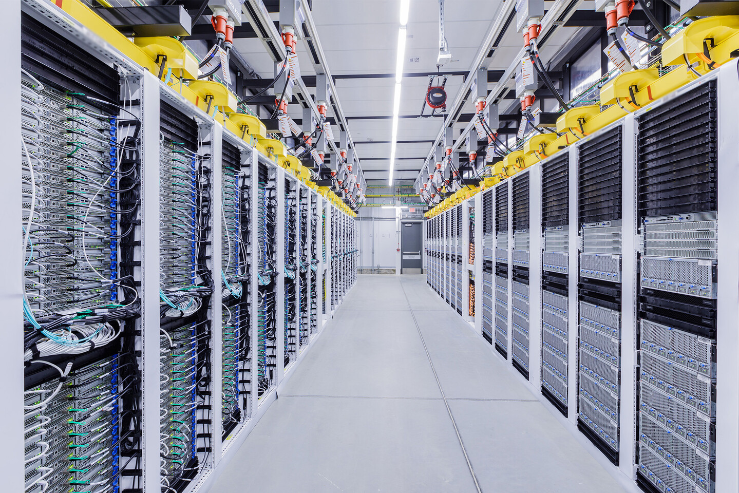
Huawei Builds Complete Domestic AI Semiconductor Supply Chain

According to the Financial Times, gathering data from satellite images and industry intelligence, Huawei has endeavored to develop a domestic AI supply chain to bypass foreign tech restriction influence. In Guanlan, China, Huawei started developing a complete facility for manufacturing semiconductors on 7 nm technology for its custom processors. Out of frustration with SMIC's low output capacity, Huawei has secured the entire silicon production, from sourcing materials, chemicals, and wafer fab equipment to chip-making equipment to actual chip design. According to Dylan Patel of SemiAnalysis, "Huawei has embarked on an unprecedented effort to develop every part of the AI supply chain domestically from wafer fabrication equipment to model building," adding, "We have never seen one company attempt to do everything before."

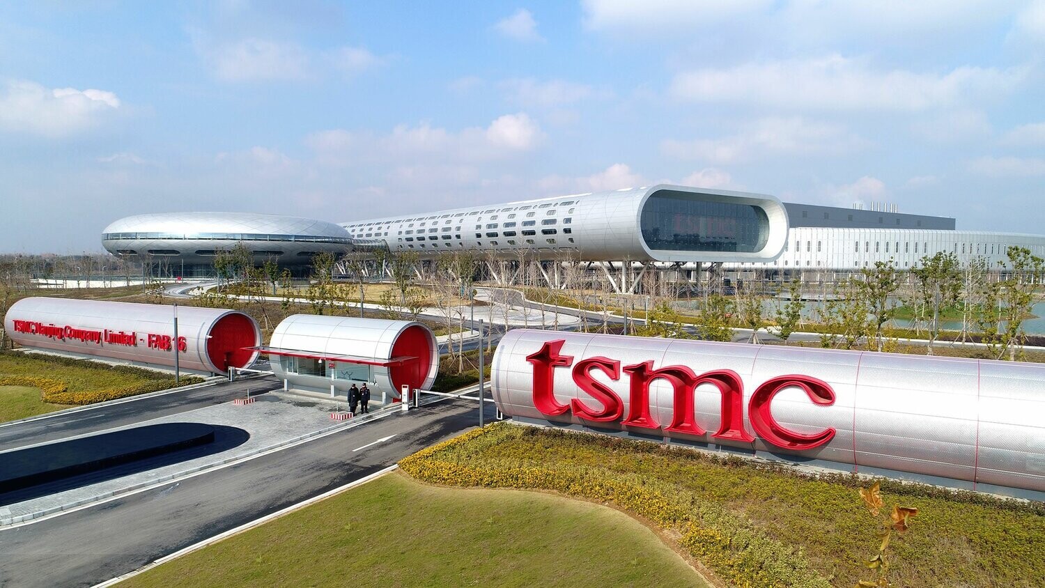
It is also reported that Huawei's rivals in silicon manufacturing, SMIC and SMEE, have deployed engineers to help Huawei develop its own manufacturing flow. A few companies, all backed by Huawei with funding and research, are the backbone of this operation. SiCarrier, which we reported on back in March, supplies optical and X-ray inspection tools, atomic force microscopes, and alignment systems for metrology; gas-based and atomic layer deposition tools for film coating; plasma etchers for patterning; rapid thermal processors for material tuning; and electrical testing platforms for reliability screening. SwaySure and Fujian Jinhua supply memory chips, Si'En and Pehgjin supply power chips, and PWX and PST deal with logic.

2024 Global Semiconductor Materials Market Posts $67.5 Billion in Revenue

Global semiconductor materials market revenue increased 3.8% to $67.5 billion in 2024, SEMI, the global industry association representing the electronics design and manufacturing supply chain, reported today in its Materials Market Data Subscription (MMDS). The recovery of the overall semiconductor market as well as the increasing demand for advanced materials for high-performance compute and high-bandwidth memory manufacturing supported 2024 materials revenue growth.

Wafer fabrication materials revenue increased 3.3% to $42.9 billion in 2024, while packaging materials revenue grew 4.7% to $24.6 billion last year. The chemical mechanical planarization (CMP), photoresist, and photoresist ancillaries segments experienced strong double-digit growth driven by increased complexity and number of processing steps required for advanced DRAM, 3D NAND flash and leading-edge logic integrated circuits (ICs). All semiconductor materials segments, except for silicon and silicon-on-insulator (SOI), registered year-on-year increases. The demand for silicon, particularly in the trailing edge segment, remained weak in 2024 as the industry continued to work through excess inventory, resulting in a 7.1% decline in silicon revenue in 2024.

TSMC Can't Track Where Its Chips End Up, Annual Report Admits

TSMC has acknowledged fundamental visibility limitations in its semiconductor supply chain, stating in its latest annual report that it "inherently lacks visibility regarding the downstream use or user of final products." This disclosure relates to an incident where 7 nm chips manufactured for Sophgo were later identified in Huawei's Ascend 910B/C AI accelerators, whose hardware is subject to US export restrictions. The contract foundry outlined its standard process: receiving GDS files through intermediaries, validating technical specifications, creating photomasks, and fabricating wafers without insight into end applications. Subsequent analysis revealed that those very chips matched Huawei's specifications, providing components for approximately one million dual‑chiplet AI accelerator units, with two million dies shipped to Huawei.

The report warns that compliance violations by supply‑chain partners, such as failing to secure proper import, export or re‑export permits, could trigger regulatory investigations and penalties, even when TSMC adheres to its established protocols. US already proposed a $1 billion fine for TSMC. This visibility gap just shows that challenges in semiconductor manufacturing, where complex distribution networks obscure the path between fabrication and deployment, are not easily overcome. Foundries are facing increasing pressure to enhance tracking capabilities despite the inherent limitations of the contract manufacturing model. US sanctions on Chinese companies are growing their walls even higher, and this could mean that sanction-abiding companies might avoid doing business with Chinese entities altogether to avoid getting fined.

Report Suggests Huawei Ascend 910C AI Accelerator's Utilization of Foreign Parts; Investigators Find 7 nm TSMC Dies

Earlier today, TechPowerUp covered the alleged performance prowess of Huawei's CloudMatrix 384 system super node. According to SemiAnalysis opinion, the system's Ascend 910C AI accelerators are a generation behind—in terms of chip performance—when compared to NVIDIA's GB200 "Blackwell" AI GPU design. SMIC seemed to be in the picture, as Huawei's main fabrication partner—possibly with an in-progress 5 nm node process. Instead, SemiAnalysis has surmised that the Ascend 910C is based on plenty of non-native technologies. Huawei's (current and prior) "aggressive skirting of export controls" has likely enabled the new-gen AI chip's better than expected performance stats. SemiAnalysis documented the early sample's origins: "while the Ascend chip can be fabricated at SMIC, we note that this is a global chip that has HBM from Korea (Samsung), primary wafer production from TSMC (Taiwan), and is fabricated by 10s of billions of wafer fabrication equipment from the US, Netherlands, and Japan...One common misconception is that Huawei's 910C is made in China. It is entirely designed there, but China still relies heavily on foreign production."

Despite China's premiere foundry business making pleasing in-roads with a theorized "7 nm N+2" manufacturing test line, Huawei has seemingly grown impatient with native immature production options. Today's SemiAnalysis article presents a decent dose of inside knowledge: "while SMIC does have 7 nm, the vast majority of Ascend 910B and 910C are made with TSMC's 7 nm. In fact, the US Government, TechInsights, and others have acquired Ascend 910B and 910C and every single one used TSMC dies. Huawei was able to circumvent the sanctions on them against TSMC by purchasing ~$500 million of 7 nm wafers through another company, Sophgo...It is rumored Huawei continues to receive wafers from TSMC via another 3rd party firm, but we cannot verify this rumor." Another (fabless) Chinese chip design firm—Xiaomi—appears to still have direct/unrestricted access to TSMC manufacturing lines, albeit not for enterprise-grade AI products.

TSMC Reportedly Preparing New Equipment for 1.4 nm Trial Run at "P2" Baoshan Plant

Industry insiders posit that TSMC's two flagship fabrication facilities are running ahead of schedule with the development of an advanced 2 nm (N2) process node. A cross-facility mass production phase is tipped to begin later this year, which leaves room for next-level experiments. Taiwan's Economic Daily News has heard supply chain whispers about the Baoshan "P2" plant making internal preparations for a truly cutting edge 1.4 nm-class product. According to the report, unnamed sources have claimed that: "TSMC has made a major breakthrough in the advancement of its 1.4 nm process. (The company) has recently notified suppliers to prepare the necessary equipment for 1.4 nm, and plans to install a trial production 'mini-line' at P2 (Baoshan Fab 20)."

Their Hsinchu-adjacent "Fab 20" site is touted as a leading player in the prototyping of this new technology. Industry moles reckon that "1.4 nm expertise" will eventually trickle over to nearby "P3 and P4 plants" for full production phases. Allegedly, these factories were originally going to be involved in the manufacturing of 2 nm (N2) wafers. Additionally, TSMC's "Fab 25" campus could potentially play host to trial 1.4 nm activities—the Economic Daily News article proposes that four plants based in the Central Taiwan Science Park are pitching in with collaborative work. As interpreted by TrendForce, "P1" could begin "risk trial production" by 2027, followed by full-scale output within the following year.

Report Suggests TSMC's Successful Completion of 2 nm Trial Phase, Cross-facility Mass Production Expected by End of Year

Going back to the start of this year, TSMC's trial run of a cutting-edge 2 nm (N2) node process was reportedly progressing beyond initial expectations. According to industry moles, two flagship fabrication facilities are "optimistically" tipped to pump out 80,000 units per month (by the end of 2025). This cross-facility total figure was linked to TSMC's Baoshan—located near the Northern Taiwanese city of Hsinchu—and Kaohsiung (in the South) plants. The latest regional reports suggest that the aforementioned trial phase was a resounding success, with pleasing results pointing to an "ahead of schedule" transfer to mass production phases. Insiders previously heard about the Kaohsiung production hub's schedule; with mass production set to start by early 2026—according to fresh rumors, revised calendars have a kick-off window repositioned somewhere in late 2025. Apparently a special "2 nm plant expansion ceremony" took place in that location, earlier today.

A noted semiconductor business analyst—Ming-Chi Kuo—reckons that recent 2 nm pilot yields have progressed well over the 60% mark, meaning that the involved foundry teams are more than ready to move onto kicking things into high gear. Taiwan's Economic News Daily anticipates significant financial gains, due to TSMC N2 products already being in high demand: "the quarterly revenue in the second half of the year is expected to reach one trillion yuan (~US$30.1 billion) for the first time, and it is poised to challenge the goal of earning twice the share capital in a quarter and rewrite the record for a single quarter." The local publication claims that TSMC Baoshan's "first batch of production capacity" is fully reserved for Apple, while Kaohsiung will take care of orders for other (i.e. less) important customers.

China Doubles Down on Semiconductor Research, Outpacing US with High-Impact Papers

When the US imposed sanctions on Chinese semiconductor makers, China began the push for sovereign chipmaking tools. According to a study conducted by the Emerging Technology Observatory (ETO), Chinese institutions have dramatically outpaced their US counterparts in next-generation chipmaking research. Between 2018 and 2023, nearly 475,000 scholarly articles on chip design and fabrication were published worldwide. Chinese research groups contributed 34% of the output—compared to just 15% from the United States and 18% from Europe. The study further emphasizes the quality of China's contributions. Focusing on the top 10% of the most-cited articles, Chinese researchers were responsible for 50% of this high-impact work, while American and European research accounted for only 22% and 17%, respectively.

This trend shows China's lead isn't about numbers only, and suggests that its work is resonating strongly within the global academic community. Key research areas include neuromorphic, optoelectric computing, and, of course, lithography tools. China is operating mainly outside the scope of US export restrictions that have, since 2022, shrunk access to advanced chipmaking equipment—precisely, tools necessary for fabricating chips below the 14 nm process node. Although US sanctions were intended to limit China's access to cutting-edge manufacturing technology, the massive body of Chinese research suggests that these measures might eventually prove less effective, with Chinese institutions continuing to push forward with influential, high-citation studies. However, Chinese theoretical work is yet to be proven in the field, as only a single company currently manufactures 7 nm and 5 nm nodes—SMIC. Chinese semiconductor makers still need more advanced lithography solutions to reach high-volume manufacturing on more advanced nodes like 3 nm and 2 nm to create more powerful domestic chips for AI and HPC.

Chinese Mature Nodes Undercut Western Silicon Pricing, to Capture up to 28% of the Market This Year

Chinese manufacturers have seized significant market share in legacy chip production, driving prices down and creating intense competitive pressure that Western competitors cannot match. The so-called "China shock" in the semiconductor sector appears as mature node production shifts East at accelerating rates. Legacy process nodes, which are usually 16/20/22/24 nm and larger, form the backbone of consumer electronics and automotive applications while providing established manufacturers with stable revenue streams for R&D investment. However, this economic framework now faces structural disruption as Chinese fabs leverage domestic demand and government support to expand capacity. By Q4 2025, Chinese facilities will control 28% of global mature chip production, with projections indicating further expansion to 39% by 2027.

This rapid capacity growth directly results from Beijing's strategic pivot following US export controls on advanced semiconductor equipment, which redirected investment toward mature nodes where technological barriers remain lower. This is happening in parallel with companies like SMIC, although isolated, which are developing lithography solutions for cutting-edge 5 nm and 3 nm wafer production. For older nodes, The market impact appears most pronounced in specialized materials like silicon carbide (SiC). Industry benchmark 6-inch SiC wafers from Wolfspeed were previously $1,500, compared to current $500 pricing from Guangzhou Summit Crystal Semiconductor—representing a 67% price compression that Western manufacturers cannot profitably match. Multiple semiconductor firms report significant financial strain from this pricing pressure. Wolfspeed has implemented 20% workforce reductions following a 96% market capitalization decline, while Onsemi recently announced 9% staff cuts. With more Chinese expansion into the mature node category, Western companies can't keep up with the lowered costs of what is now becoming a commodity.

China's Semiconductor Equipment Spending to Decline in 2025, First Decline in Recent Years

China's dominance in semiconductor equipment procurement is expected to face its first setback since 2021, with spending projected to decrease from $41 billion to $38 billion in 2025, according to semiconductor research firm TechInsights. This 6% decline marks a significant shift for the world's largest buyer of wafer fabrication equipment, whose purchases represented 40% of global sales in 2024. The downturn reflects mounting pressures from both market dynamics and geopolitical constraints. US export controls targeting advanced semiconductor capabilities have intensified while domestic chipmakers grapple with overcapacity in mature node segments. SMIC, China's leading foundry, has already signaled concerns about oversupply risks in this sector, where Chinese manufacturers have rapidly expanded their market share against Taiwanese competitors.

Despite these headwinds, Chinese equipment manufacturers have notably advanced domestic capability development. Naura Technology Group has emerged as the seventh-largest global equipment manufacturer, while AMEC continues to expand its international presence. However, critical gaps persist in China's semiconductor equipment ecosystem, particularly in lithography systems, where dependence on foreign suppliers like ASML remains high. TechInsights data reveals that Chinese companies supplied only 17% of testing tools and 10% of domestic assembly equipment in 2023. The spending reduction comes after a period of aggressive stockpiling prompted by US sanctions to limit Beijing's access to advanced chipmaking capabilities, especially those applicable to artificial intelligence and military applications. However, Chinese manufacturers have demonstrated resilience, with SMIC and Huawei successfully producing advanced chips through alternative, albeit more costly, manufacturing methods.

Report Suggests OpenAI Finalizing Proprietary GPU Design

Going back a year, we started hearing about an OpenAI proprietary AI chip project—this (allegedly) highly ambitious endeavor included grand plans for a dedicated fabrication network. TSMC was reportedly in the equation, but indirectly laughed at the AI research organization's ardent requests. Fast-forward to the present day; OpenAI appears to be actively pursuing a proprietary GPU design through traditional means. A Reuters exclusive report points to 2025 being an important year for the company's aforementioned "in-house" AI chip—the publication believes that OpenAI's debut silicon design has reached the finalization stage. Insiders have divulged that the project is only months away from being submitted to TSMC for "taping out." The foundry's advanced 3-nanometer process technology is reported to be on the cards. A Reuters source reckons that the unnamed chip features: "a commonly used systolic array architecture with high-bandwidth memory (HBM)...and extensive networking capabilities."

Broadcom is reportedly assisting with the development of OpenAI's in-house design—we heard about rumored negotiations taking place last summer. Jim Keller's tempting offer—of creating an AI chip for less than $1 trillion—was ignored early last year; OpenAI has instead assembled its own internal team of industry veterans. The October 2024 news cycle posited that former Google TPU engineers were drafted in as team leaders, with a targeted mass production window scheduled for 2026. The latest Reuters news article reiterates this projected timeframe, albeit dependent on the initial tape going "smoothly." OpenAI's chip department has grown to around forty individuals with recent months, according to industry moles—a small number relative to the headcounts at "Google or Amazon's AI chip program."

TSMC Reportedly Ahead of Schedule with 2 nm Trial Production at Kaohsiung Fab

TSMC is reportedly making decent progress with its advanced 2 nm (N2) node—industry news pieces from earlier this month pointed to the initiation of production lines across three fabrication sites. Taiwan's Economic Daily News has kept close tabs on these trial runs—insiders have indicated that TSMC's Kaohsiung plant is capable of matching the Baoshan location's targeted manufacturing output (5000 wafers per month, 60 percent yield). Reports suggest that the Kaohsiung 2 nm trial production will start up later this month—much earlier than anticipated.

The Taiwanese chip foundry giant is taking on the challenge of meeting "greater than expected" demand for its new generation 2 nm product—TSMC chairman C.C. Wei has previously stated that its latest and greatest is more popular (pre-launch) with customers than older 3 nm lines. Apple is rumored to be first in line—not a big surprise since TSMC has (supposedly) rolled out the VVIP red carpet for them in recent times. The Economic Daily News article also mentions Qualcomm and MediaTek being next in the queue for N2. TSMC's best foundries are expected to initiate mass production by the end of 2025.

Intel Foundry Unveils Technology Advancements at IEDM 2024

Today at the IEEE International Electron Devices Meeting (IEDM) 2024, Intel Foundry unveiled new breakthroughs to help drive the semiconductor industry forward into the next decade and beyond. Intel Foundry showcased new material advancements that help improve interconnections within a chip, resulting in up to 25% capacitance by using subtractive ruthenium. Intel Foundry also was first to report a 100x throughput improvement using a heterogeneous integration solution for advanced packaging to enable ultra-fast chip-to-chip assembly. And to further drive gate-all-around (GAA) scaling, Intel Foundry demonstrated work with silicon RibbonFET CMOS and with gate oxide module for scaled 2D FETs for improved device performance.

"Intel Foundry continues to help define and shape the roadmap for the semiconductor industry. Our latest breakthroughs underscore the company's commitment to delivering cutting-edge technology developed in the U.S., positioning us well to help balance the global supply chain and restore domestic manufacturing and technology leadership with the support of the U.S. CHIPS Act," says Sanjay Natarajan, Intel senior vice president and general manager of Intel Foundry Technology Research.

Broadcom Delivers Industry's First 3.5D F2F Technology for AI XPUs

Broadcom Inc. today announced the availability of its 3.5D eXtreme Dimension System in Package (XDSiP) platform technology, enabling consumer AI customers to develop next-generation custom accelerators (XPUs). The 3.5D XDSiP integrates more than 6000 mm² of silicon and up to 12 high bandwidth memory (HBM) stacks in one packaged device to enable high-efficiency, low-power computing for AI at scale. Broadcom has achieved a significant milestone by developing and launching the industry's first Face-to-Face (F2F) 3.5D XPU.

The immense computational power required for training generative AI models relies on massive clusters of 100,000 growing to 1 million XPUs. These XPUs demand increasingly sophisticated integration of compute, memory, and I/O capabilities to achieve the necessary performance while minimizing power consumption and cost. Traditional methods like Moore's Law and process scaling are struggling to keep up with these demands. Therefore, advanced system-in-package (SiP) integration is becoming crucial for next-generation XPUs. Over the past decade, 2.5D integration, which involves integrating multiple chiplets up to 2500 mm² of silicon and HBM modules up to 8 HBMs on an interposer, has proven valuable for XPU development. However, as new and increasingly complex LLMs are introduced, their training necessitates 3D silicon stacking for better size, power, and cost. Consequently, 3.5D integration, which combines 3D silicon stacking with 2.5D packaging, is poised to become the technology of choice for next-generation XPUs in the coming decade.

Infineon and Quantinuum Partner to Advance Quantum Computing

Infineon Technologies AG, a global leader in semiconductor solutions, and Quantinuum, a global leader in integrated, full-stack quantum computing, today announced a strategic partnership to develop the future generation of ion traps. This partnership will drive the acceleration of quantum computing and enable progress in fields such as generative chemistry, material science, and artificial intelligence.

"We are thrilled to partner with Quantinuum, a leader in quantum computing, to push the boundaries of quantum computing and generate larger, more powerful machines that solve meaningful real-life problems," said Richard Kuncic, Senior Vice President and General Manager Power Systems at Infineon Technologies. "This collaboration brings together Infineon's state-of-the-art knowledge in process development, fabrication, and quantum processing unit (QPU) technology with Quantinuum's cutting-edge ion-trap design expertise and experience with operating high-performance commercial quantum computers."

xMEMS Introduces 1mm-Thin Active Micro-Cooling Fan on a Chip

xMEMS Labs, developers of the foremost platform for piezoMEMS innovation and creators of the world's leading all-silicon micro speakers, today announced its latest industry-changing innovation: the xMEMS XMC-2400 µCooling chip, the first-ever all-silicon, active micro-cooling fan for ultramobile devices and next-generation artificial intelligence (AI) solutions.

For the first time, with active, fan-based micro-cooling (µCooling) at the chip level, manufacturers can integrate active cooling into smartphones, tablets, and other advanced mobile devices with the silent, vibration-free, solid-state xMEMS XMC-2400 µCooling chip, which measures just 1-millimeter thin.

Texas Instruments to Receive up to $1.6 billion in CHIPS Act Funding for Semiconductor Manufacturing Facilities in Texas and Utah

Texas Instruments (TI) (Nasdaq: TXN) and the U.S. Department of Commerce have signed a non-binding Preliminary Memorandum of Terms for up to $1.6 billion in proposed direct funding under the CHIPS and Science Act to support three 300 mm wafer fabs already under construction in Texas and Utah. In addition, TI expects to receive an estimated $6 billion to $8 billion from the U.S. Department of Treasury's Investment Tax Credit for qualified U.S. manufacturing investments. The proposed direct funding, coupled with the investment tax credit, would help TI provide a geopolitically dependable supply of essential analog and embedded processing semiconductors.

"The historic CHIPS Act is enabling more semiconductor manufacturing capacity in the U.S., making the semiconductor ecosystem stronger and more resilient," said Haviv Ilan, president and CEO of Texas Instruments. "Our investments further strengthen our competitive advantage in manufacturing and technology as we expand our 300 mm manufacturing operations in the U.S. With plans to grow our internal manufacturing to more than 95% by 2030, we're building geopolitically dependable, 300 mm capacity at scale to provide the analog and embedded processing chips our customers will need for years to come."

Imec Develops Ultra-Low Noise Si MOS Quantum Dots Using 300mm CMOS Technology

Imec, a world-leading research and innovation hub in nanoelectronics and digital technologies, today announced the demonstration of high quality 300 mm-Si-based quantum dot spin qubit processing with devices resulting in a statistically relevant, average charge noise of 0.6µeV/√ Hz at 1 Hz. In view of noise performance, the values obtained are the lowest charge noise values achieved on a 300 mm fab-compatible platform.

Such low noise values enable high-fidelity qubit control, as reducing the noise is critical for maintaining quantum coherence and high fidelity control. By demonstrating those values, repeatedly and reproducibly, on a 300 mm Si MOS quantum dot process, this work makes large-scale quantum computers based on Si quantum dots a realistic possibility.

Quinas Receives £1.1m to Enable Industrialisation of ULTRARAM

An Innovate UK project worth £1.1M has been awarded to the Lancaster University spinout firm Quinas, the global semiconductor company IQE and Lancaster and Cardiff Universities. Quinas will coordinate the ambitious project which is the first step towards volume production of the universal computer memory ULTRARAM invented by Lancaster Physics Professor Manus Hayne.

ULTRARAM has extraordinary properties, combining the non-volatility of a data storage memory, like flash, with the speed, energy-efficiency, and endurance of a working memory, like DRAM. Most of the funding for the one-year project will be spent at IQE which will scale up the manufacture of compound semiconductor layers from Lancaster University to an industrial process at the Cardiff based firm. This will involve IQE developing advanced capability for growth of the compound semiconductors gallium antimonide and aluminium antimonide for the first time. The project follows significant investment to boost the UK semiconductor industry and the establishment of the world's first compound semiconductor cluster in South Wales.

Report: Only 10% of TSMC's Capacity will Come from Non-Taiwan Fabs

A recent report from Taiwan TV News has revealed that TSMC's overseas expansion plans will only contribute around 10% of the company's total silicon production capacity. TSMC's overseas expansion strategy has been a topic of significant interest in the tech industry as the company seeks to diversify its manufacturing capabilities beyond its home base in Taiwan. The company has announced plans to build new fabrication plants in the United States, Japan, and potentially other regions in an effort to mitigate supply chain risks and better serve its global customer base. However, according to the report, these overseas facilities will only account for a small fraction of 10% of TSMC's overall production capacity.

The majority of the company's manufacturing will continue to be centered in Taiwan, where it maintains its most advanced and high-volume fabs. There are also significant challenges and investments required to establish new semiconductor manufacturing facilities overseas. Building a state-of-the-art fab can cost billions of dollars and take several years to complete, making it a complex and capital-intensive undertaking. Despite the relatively small contribution of its overseas facilities, TSMC's global expansion is still seen as a crucial step in diversifying its supply chain and mitigating geopolitical risks. The company's ability to maintain its technological leadership and meet the growing demand for advanced chips will be crucial in the years to come.

Intel and Apollo Agree to Joint Venture Related to Intel's Fab 34 in Ireland

Intel Corporation (Nasdaq: INTC) and Apollo (NYSE: APO) today announced a definitive agreement under which Apollo-managed funds and affiliates will lead an investment of $11 billion to acquire from Intel a 49% equity interest in a joint venture entity related to Intel's Fab 34. The transaction represents Intel's second Semiconductor Co-Investment Program (SCIP) arrangement. SCIP is an element of Intel's Smart Capital strategy, a funding approach designed to create financial flexibility to accelerate the company's strategy, including investing in its global manufacturing operations, while maintaining a strong balance sheet.

Located in Leixlip, Ireland, Fab 34 is Intel's leading-edge high-volume manufacturing (HVM) facility designed for wafers using the Intel 4 and Intel 3 process technologies. To date, Intel has invested $18.4 billion in Fab 34. This transaction allows Intel to unlock and redeploy to other parts of its business a portion of this investment while continuing the build-out of Fab 34. As part of its transformation strategy, Intel has committed billions of dollars of investments to regaining process leadership and building out leading-edge wafer fabrication and advanced packaging capacity globally.

STMicroelectronics to Build the World's First Fully Integrated Silicon Carbide Facility in Italy

STMicroelectronics, a global semiconductor leader serving customers across the spectrum of electronics applications, announces a new high-volume 200 mm silicon carbide ("SiC") manufacturing facility for power devices and modules, as well as test and packaging, to be built in Catania, Italy. Combined with the SiC substrate manufacturing facility being readied on the same site,these facilities will form ST's Silicon Carbide Campus, realizing the Company's vision of a fully vertically integrated manufacturing facility for the mass production of SiC on one site.The creation of the new Silicon Carbide Campus is a key milestone to support customers for SiC devices across automotive, industrial and cloud infrastructure applications, as they transition to electrification and seek higher efficiency.

"The fully integrated capabilities unlocked by the Silicon Carbide Campus in Catania will contribute significantly to ST's SiC technology leadership for automotive and industrial customers through the next decades," said Jean-Marc Chery, President and Chief Executive Officer of STMicroelectronics. "The scale and synergies offered by this project will enable us to better innovate with high-volume manufacturing capacity, to the benefit of our European and global customers as they transition to electrification and seek more energy efficient solutions to meet their decarbonization goals."
STMicroelectronics Italy

China Launches Massive $47.5 Billion "Big Fund" to Boost Domestic Chip Industry

Beijing has doubled down on its push for semiconductor self-sufficiency with the establishment of a new $47.5 billion investment fund to accelerate growth in the domestic chip sector. The fund, officially registered on May 24th under the name "China Integrated Circuit Industry Investment Fund Phase III", represents the largest of three state-backed vehicles aimed at cultivating China's semiconductor capabilities. The announcement comes as tensions over advanced chip technology continue to escalate between the U.S. and China. Over the past couple years, Washington has steadily ratcheted up export controls on semiconductors to Beijing over national security concerns about potential military applications. These measures have lent new urgency to China's quest for self-sufficiency in chip design and manufacturing.

With a war chest of 344 billion yuan ($47.5 billion), the "Big Fund" dwarfs the combined capital of the first two semiconductor investment vehicles launched in 2014 and 2019. Officials have outlined a multipronged strategy targeting key bottlenecks, focusing on equipment for chip fabrication plants. The fund has bankrolled major projects such as flash memory maker Yangtze Memory Technologies and leading foundries like SMIC and Huahong. China's homegrown chip industry still needs to catch up to global leaders like Intel, Samsung, and TSMC. However, the immense scale of state-directed capital illustrates Beijing's unwavering commitment to developing a self-reliant supply chain for semiconductors—a technology viewed as indispensable for economic and military competitiveness. News of the "Big Fund" sent Chinese chip stocks surging over 3% on hopes of fresh financing tailwinds.

Toshiba Completes New 300-Millimeter Wafer Fabrication Facility for Power Semiconductors

Toshiba Electronic Devices & Storage Corporation ("Toshiba") today held a ceremony to mark the completion of a new 300-millimeter wafer fabrication facility for power semiconductors and an office building at Kaga Toshiba Electronics Corporation in Ishikawa Prefecture, Japan, one of Toshiba's key group companies. The completion of construction is a major milestone for Phase 1 of Toshiba's multi-year investment program. Toshiba will now proceed with equipment installation, toward starting mass production in the second half of fiscal year 2024. Once Phase 1 reaches full-scale operation, Toshiba's production capacity for power semiconductors, mainly MOSFETs and IGBTs, will be 2.5 times that of fiscal 2021, when the investment plan was made. Decisions on the construction and start of operation of Phase 2 will reflect market trends.

The new manufacturing building follows and will make a major contribution to Toshiba's Business Continuity Plan (BCP): it has a seismic isolation structure that absorbs earthquake shock and redundant power sources. Energy from renewable source and solar panels on the roof of the building (onsite PPA model) will allow the facility to meet 100% of its power requirement with renewable energy.

TSMC to Introduce Location Premium for Overseas Chip Production

As a part of its Q1 earnings call discussion, one of the largest semiconductor manufacturers, TSMC, has unveiled a strategic move to charge a premium for chips manufactured at its newly established overseas fabrication plants. During an earnings call, TSMC's CEO, C.C. Wei, announced that the company will impose higher pricing for chips produced outside Taiwan to offset the higher operational costs associated with these international locations. This move aims to maintain TSMC's target gross margin of 53% amidst rising expenses such as inflation and elevated electricity costs. This decision comes as TSMC expands its global footprint with new facilities in the United States, Germany, and Japan (JAMS) to meet the increasing demand for semiconductor chips worldwide. The company's new US-based Arizona facility, known as Fab 21, has faced delays due to equipment installation issues and labor negotiations.

Chips produced at this site, utilizing TSMC's advanced N5 and N4 nodes, could cost between 20% to 30% more than those manufactured in Taiwan. TSMC's strategy to manage the cost disparities across different geographic locations involves strategic pricing, securing government support, and leveraging its manufacturing technology leadership. This approach reflects the company's commitment to maintaining its competitive edge while navigating the complexities of global semiconductor manufacturing in today's fragmented market. Introducing a location premium is expected to impact American semiconductor designers, who may need to pass these costs on to specific market segments, particularly those with lower price sensitivity, such as government-related projects. Despite these challenges, TSMC's overseas expansion underscores its adaptive strategies in the face of global economic pressures and industry demands, ensuring its continued position as a leading player in the semiconductor industry.

SK hynix Signs Investment Agreement of Advanced Chip Packaging with Indiana

SK hynix Inc., the world's leading producer of High-Bandwidth Memory (HBM) chips, announced today that it will invest an estimated $3.87 billion in West Lafayette, Indiana to build an advanced packaging fabrication and R&D facility for AI products. The project, the first of its kind in the United States, is expected to drive innovation in the nation's AI supply chain, while bringing more than a thousand new jobs to the region.

The company held an investment agreement ceremony with officials from Indiana State, Purdue University, and the U.S. government at Purdue University in West Lafayette on the 3rd and officially announced the plan. At the event, officials from each party including Governor of Indiana Eric Holcomb, Senator Todd Young, Director of the White House Office of Science and Technology Policy Arati Prabhakar, Assistant Secretary of Commerce Arun Venkataraman, Secretary of Commerce State of Indiana David Rosenberg, Purdue University President Mung Chiang, Chairman of Purdue Research Foundation Mitch Daniels, Mayor of city of West Lafayette Erin Easter, Ambassador of the Republic of Korea to the United States Hyundong Cho, Consul General of the Republic of Korea in Chicago Junghan Kim, SK vice chairman Jeong Joon Yu, SK hynix CEO Kwak Noh-Jung and SK hynix Head of Package & Test Choi Woojin, participated.
Return to Keyword Browsing
Jun 9th, 2025 14:36 EEST change timezone

New Forum Posts

Popular Reviews

TPU on YouTube

Controversial News Posts